最新情報

NanoWorld ACTIVE SELF-ASSEMBLY OF PIEZOELECTRIC BIOMOLECULAR FILMS VIA SYNERGISTIC NANOCONFINEMENT AND IN-SITU POLING - news

ACTIVE SELF-ASSEMBLY OF PIEZOELECTRIC BIOMOLECULAR FILMS VIA SYNERGISTIC NANOCONFINEMENT AND IN-SITU POLINGWed Feb 21 2024

Active self-assembly of piezoelectric biomolecular films via synergistic nanoconfinement and in-situ poling
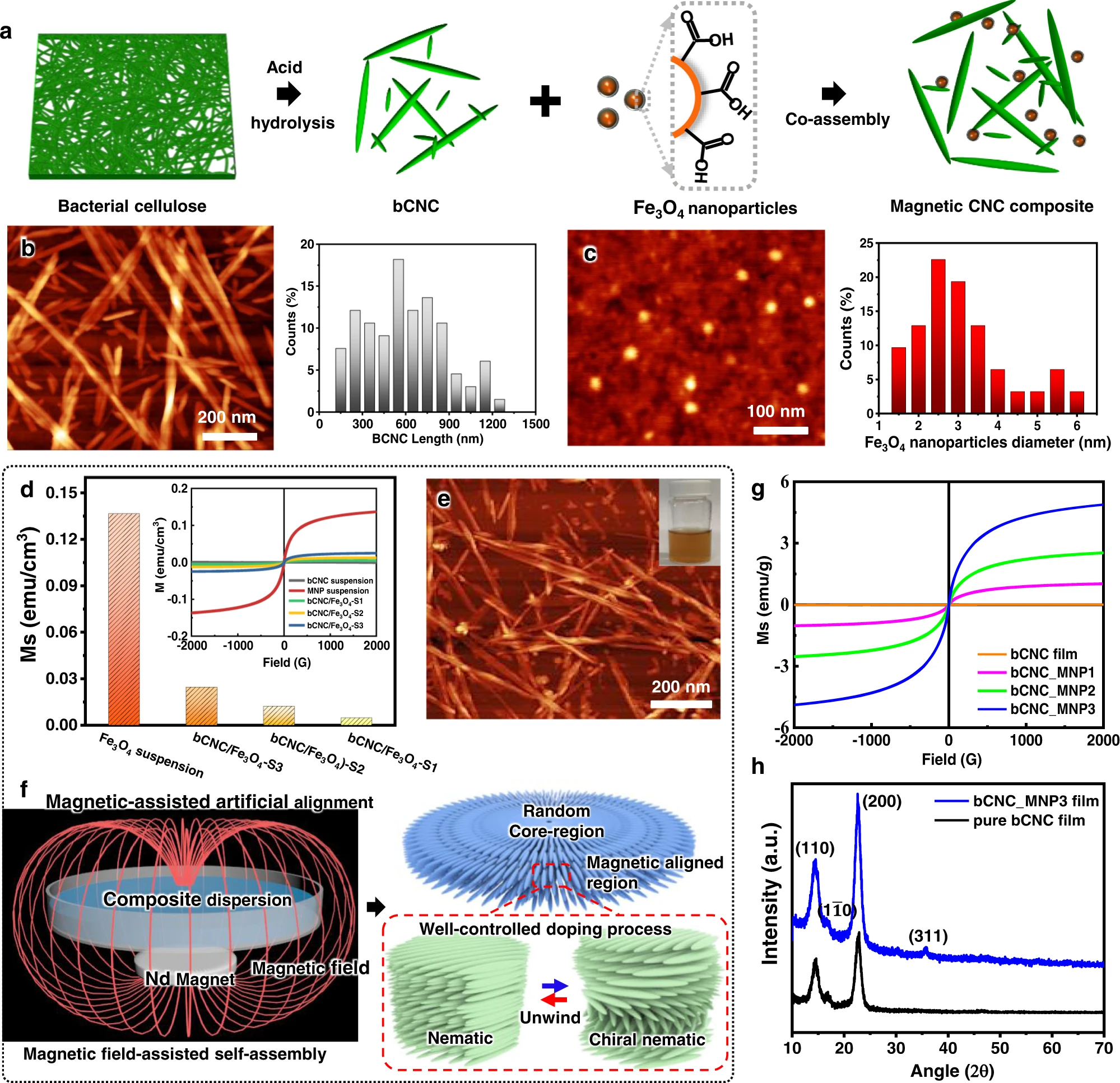
Piezoelectric biomaterials have attracted great attention owing to the recent recognition of the impact of piezoelectricity on biological systems and their potential applications in implantable sensors, actuators, and energy harvesters. However, their practical use is hindered by the weak piezoelectric effect caused by the random polarization of biomaterials and the challenges of large-scale alignment of domains.* In the article “Active self-assembly of piezoelectric biomolecular films via synergistic nanoconfinement and in-situ poling” Zhuomin Zhang, Xuemu Li, Zehua Peng, Xiaodong Yan, Shiyuan Liu, Ying Hong, Yao Shan, Xiaote Xu, Lihan Jin, Bingren Liu, Xinyu Zhang, Yu Chai, Shujun Zhang, Alex K.-Y. Jen […]

MikroMasch Nanoendoscopy AFM is performed with modified OPUS 240AC-NG AFM probes

Nanoendoscopy AFM is performed with modified OPUS 240AC-NG AFM probes.Tue Feb 20 2024

Protocol for live imaging of intracellular nanoscale structures using atomic force microscopy with nanoneedle probes
“Atomic force microscopy (AFM) is capable of nanoscale imaging but has so far only been used on cell surfaces when applied to a living cell. Here, we describe a step-by-step protocol for nanoendoscopy-AFM, which enables the imaging of nanoscale structures inside living cells. The protocol consists of cell staining, fabrication of the nanoneedle probes, observation inside living cells using 2D and 3D nanoendoscopy-AFM, and visualization of the 3D data.”
Nanoendoscopy AFM is performed with modified OPUS 240AC-NG AFM probes.

NANOSENSORS Electron-beam lithography of nanostructures at the tips of scanning probe cantilevers - news

Electron-beam lithography of nanostructures at the tips of scanning probe cantileversFri Feb 16 2024

It is always exiting to see what our creative and innovative users are doing with our AFM probes.
In their article “Electron-beam lithography of nanostructures at the tips of scanning probe cantilevers” L. Forrer, A. Kamber, A. Knoll, M. Poggio and F. R. Braakman describe how they developed a process to fabricate nanoscale metallic gate electrodes on scanning probe cantilevers. *
They even patterned the very fragile tip of the NANOSENSORS AdvancedTEC ATEC-NC with a gate array defined through the etching process. *
Their method allows the patterning of nanoscale devices on fragile scanning probes, extending their functionality as sensors. *
Please have a look at the NANOSENSORS blog for the full citation and a direct link to the full article.

MikroMasch Lock-in Amplifier Based Peak Force Infrared Microscopy - NanoAndMore

Lock-in Amplifier Based Peak Force Infrared MicroscopyMon Jan 15 2024

Lock-in Amplifier Based Peak Force Infrared Microscopy
“[T]he current PFIR microscope requires customized hardware configuration and software programming for real-time signal acquisition and processing, which creates a high barrier to PFIR implementation. In this communication, we describe a type of lock-in amplifier-based PFIR microscopy that can be assembled with generic, commercially available equipment without special hardware or software programming.”
The measurements in PeakForce Infrared Microscopy mode are performed using our platinum coated HQ:NSC15/Pt AFM probes.

NANOSENSORS Happy Holidays from NANOSENSORS™ AFM probes - news

Happy Holidays from NANOSENSORS™ AFM probesSun Dec 24 2023

With this seasonal Special Development Christmas Tree AFM tip with a light snow coating, we would like to wish all users of our AFM probes Happy Holidays and a good start into the New Year!

We are looking forward to another year with you.

nanotools Video-Rate High-Speed-AFM To Study Permeability Barrier Within Yeast Nuclear Pore Complexes - news

Video-Rate High-Speed-AFM To Study Permeability Barrier Within Yeast Nuclear Pore ComplexesThu Dec 14 2023

Discover how nanotools QUANTUM-AC10 (Soft & Sharp) with 0.1N/m cantilevers and 2-3nm radius are applied for video-rate HS-AFM imaging of nuclear pore complexes.
https://www.nanotools.com/blog/video-rate-high-speed-afm-to-study-permeability-barrier-within-yeast-nuclear-pore-complexes.html

Title: Dynamic molecular mechanism of the nuclear pore complex permeability barrier
Authors: Toshiya Kozai, Javier Fernandez-Martinez, Trevor van Eeuwen, Paola Gallardo, Larisa E. Kapinos, Adam Mazur, Wenzhu Zhang, Jeremy Tempkin, Radhakrishnan Panatala, Maria Delgado-Izquierdo, Barak Raveh, Andrej Sali, Brian T. Chait, Liesbeth M. Veenhoff, Michael P. Rout, Roderick Y. H. Lim
Publication: bioRxiv
Pubisher: Cold Spring Harbor Laboratory
Date: April 14, 2023

NanoAndMore NanoAndMore 3D printed AFM tip scale models at 2023 MRS Fall Meeting & Exhibit

Last exhibition day at 2023 MRS Fall Meeting & ExhibitThu Nov 30 2023

Last exhibition day at 2023 MRS Fall Meeting & Exhibit Materials Research Society and the last day to have a look at our 3D printed #AFMtip scale models, find out about the many different #AFMprobes we offer and pick up some Swiss chocolate.
Opening hours today Thursday, November 30 10:00 am – 1:00 pm

NanoAndMore The second exhibition day at 2023 MRS Fall

Did you know that we now also sell the original Olympus AFM probes?Wed Nov 29 2023

It’s the second exhibition day at 2023 MRS Fall.
Did you know that we now also sell the original Olympus #AFMprobes?
Visit us today at booth # 904 to find out more.
Opening times Wednesday, November 29 10:00 am – 6:00 pm

nanotools E-AFM Nanolithography Approach Enables High-Resolution Nanopatterning - news

E-AFM Nanolithography Approach Enables High-Resolution NanopatterningThu Nov 23 2023

Discover how nanotools 500nm long, tilt compensated, high aspect ratio MCNT-500™ is applied for imaging and characterization of lithography features dimensions (depth and width).

https://www.nanotools.com/blog/e-afm-nanolithography-approach-enables-high-resolution-nanopatterning.html

Title: Electric-Field-Assisted Contact Mode Atomic Force Microscope-Based Nanolithography With Low Stiffness Conductive Probes
Authors: Zhou, H., Jiang, Y., Dmuchowski, C. M., Ke, C., and Deng, J.
Publication: Journal of Micro- and Nano-Manufacturing
Publisher: ASME International
Date: 28 April 2022

ハイライト


Loading
nanosensors-logo
nanoworld-logo
budgetsensors-logo
mikromasch-logo
opus-logo
nanotools-logo